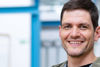
Christian Liebscher What Happens In Material Imperfections at the Atomic Level?
Christian Liebscher is Group Leader for Advanced Transmission Electron Microscopy in Structure and Nano-/Micromechanics of Materials at the Max-Planck-Institut für EisenforschungGmbH. Having completed his PhD at the University of Bayreuth, Liebscher has previously worked at University Duisburg-Essen and at the University of California, Berkley. Author of a cover story in Physical Review Letters, Liebscher was awarded with a research fellowship from the German Science Foundation (DFG) in 2013-14.
Area of Research
Material Science
since 2020
Deputy Director of Prof. Dehm
Max-Planck-Institut für Eisenforschung (more details)
Department of Structure and Nano- / Micromechanics of Materials
since 2015
Group Leader
Max-Planck-Institut für Eisenforschung (more details)
Head of the Advanced Transmission Electron Microscopy group
2014-2015
Staff Scientist
University of Duisburg-Essen (Universität Duisburg-Essen)
Interdisciplinary Center for Analytics on the Nanoscale (ICAN)
2011-2014
Postdoctoral Researcher
University of California, Berkeley
Development of novel alloy design strategies to establish hierarchical microstructures in ferritic alloys for elevated temperatu
2010-2011
Postdoctoral Researcher
University of Bayreuth (Universität Bayreuth)
Responsible for the Transmission Electron Microscopy facilities at the Chair of Metals and Alloys.
2006-2010
Ph.D.
University of Bayreuth (Universität Bayreuth)
Thesis Title: High Resolution Phase and Dislocation Analysis in Nickel Based and Platinum Based Superalloys
2000-2006
Dipl.-Ing.
University of Bayreuth (Universität Bayreuth)
Thesis Title: Microstructure as a Function of Composition of Mg-Al-Sr alloys
Fellowships
- German Science Foundation (DFG): Research fellowship (2013-2014)


Max-Planck-Institut für Eisenforschung
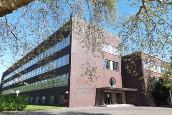
DüsseldorfNovel alloys for automotive lightweight design and airplane turbines, materials for sustainable energy conversion and storage, and the development of big data and machine learning methods – these are just a few examples of the research areas that are being investigated by the scientists of the Max-Planck-Institut für Eisenforschung. The team of engineers, material scientists, physicists, and chemists develops tailored materials and methods for mobility, energy, infrastructure, and information. To this end, the researchers study complex materials with atomic precision under real environmental conditions.
Department
Department of Structure and Nano- / Micromechanics of Materials
Plasticity, fatigue, and fracture of materials are usually initiated by local deformation processes.
The mission of the Department Structure and Nano-/Micromechanics is to develop experimental methods to perform quantitative nano-/micromechanical and tribological tests for complex and miniaturized materials,
to unravel the underlying deformation mechanisms by advanced microstructure characterization techniques from the micrometer level down to atomic dimensions, to establish material laws for local and
global mechanical behavior, and finally to generate nanostructured materials and high temperature intermetallic materials with superior mechanical properties. The in-depth microstructure investigations
include atomic resolved high-resolution (scanning) transmission electron microscopy (STEM/TEM), analytical and conventional TEM, scanning electron microscopy with electron backscattered diffraction (SEM/EBSD),
focused ion beam microscopy (FIB), X-ray diffraction and synchrotron radiation techniques. A cornerstone will be the combination of advanced characterization and mechanical testing in form of in situ nano-/micromechanical experiments which will permit to simultaneously observe the microstructural changes while measuring the mechanical response. The gained insights will be used to quantitatively describe and predict the local and global material behavior and to design superior nanostructured materials and high temperature intermetallic materials by using local confinement effects.
The synthesis of miniaturized nanostructured materials will be done by thin film deposition techniques.
Map
In electronic devices, material imperfections play a key role in determining lifespan as well as in safety considerations. In this video, CHRISTIAN LIEBSCHER puts such defects under the microscope so that we can better understand their atomic structure. Focusing on grain boundaries at which different crystals join together and using transmission electron microscopy, Liebscher explains how this research can bring about improvements in materials science and to the devices that we use in our daily lives.
LT Video Publication DOI: https://doi.org/10.21036/LTPUB10963
Observations of Grain-Boundary Phase Transformations in an Elemental Metal
- Thorsten Meiners, Timofey Frolov, Robert E. Rudd, Gerhard Dehm and Christian H. Liebscher
- Nature
- Published in 2020


